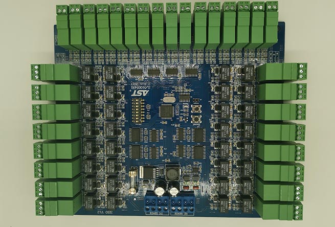
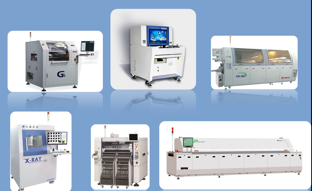
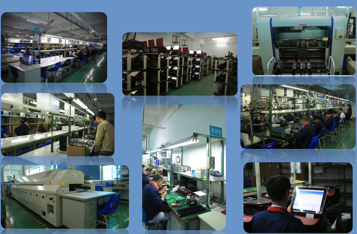
● 4 YAMAHA High-speed SMT Lines
● 6 million daily SMT placements capability
● 400,000 daily DIP placements capability
● 500×600 mm Maximum Board Size
● 0.25"x 0.25" Minimum Board Size
● 450 mm Max. Width for Wave-Solder
● Passives Components Down to 0201 Size BGA and VFBGA Leadless Chip Carrier/CSP Double-Sided SMT Assembly Fine Pitch to 08 Mil BGA Repair and ReballPart Removal and Replacement
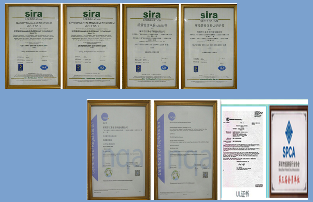
SMT and DIP/X-RAY Inspection/AOI Testing/In-circuit-test (ICT)/Flying Probe/Function Test/Burn-in/Finished products assembly
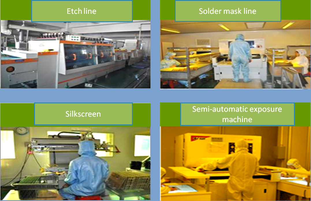
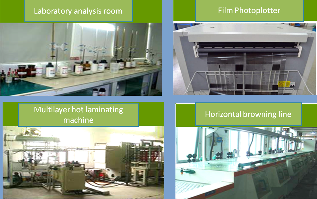
PCB processing capability
| PCB service | Process capability |
| Layer | 1-20 layers |
| Maximum size | ≤600*500mm |
| Thickness | 0.1-5.0mm |
| Wire copper foil thickness | 17-343um(10oz) |
| Minimum linewidth / line distance | 0.075/0.065mm(3mil/2.8mil) |
| Minimum aperture | 0.15mm(6mil) |
| Minimum welding pad | 0.2mm(8mil) |
| Impedance control | +/-10% |
| Shape processing accuracy | +/-0.10mm(4mil) |
| Board type | FR-4, aluminum - base, copper -base, ROGERS, ARLON, Teflon, composite |
| Surface treatment | Tin spray, ENIG, Immerse Au, immersion silver, im mersion tin, osp, gold osp, electrospray tin |
PCB ASSEMBLY CAPABILITY
| SMT service | Process capability |
| Processing type | SMT, DIP, After welding, test |
| Maximum board | L50×W50mm~L510×W460mm |
| Maximum thickness | 3mm |
| Minimum thickness | 0.5mm |
| Minimum component | 1005 |
| Maximum component size | 150mm*150mm |
| Minimum pin component spacing | 0.3mm |
| Minimum bga spacing | 0.3mm |
| Maximum component mounting accuracy(100FP) | Whole assembly accuracy up to ±50 micron,whole process repetition accuracy ±30 micron. |
| SMT capacity | 4 million pins / day |
| DIP capacity | 100 thousand/ day |