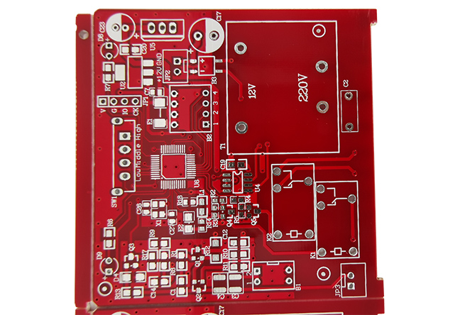
Brand Name: OEM pcb design
Model Number: OEM
Base Material: FR4
Copper Thickness: 1/3oz-12oz
Board Thickness: 0.15-4.5mm
Min. Hole Size: 0.1mm
Min. Line Width: 3.5mil
Min. Line Spacing: 3.5mil
Surface Finishing: ENIG,HAL LF,OSP, Immersion Ag
Layer: 1-48 layer
Solder mask color: Green,Red, Black, Yellow, Blue,white
Max Board Size: 610X915mm
Min board size: 10x10mm
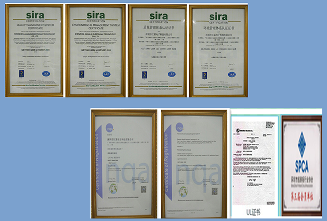
Certificate: ISO9001/Iso14001/CE/ROHS
Usage: OEM Electronics
Testing Service: 100% E-testing
Standard: IPC class II-III
Analysis of some phenomenon in PCB fabrication:
Issue: virtual welding, continuous welding, leakage welding
Result analysis:
(1) The amount of flux coating is too small or uneven;
(2) Some of the pads or solder fillets are heavily oxidized;
(3) The PCB design is unreasonable;
(4) The clogged foaming tube and the uneven foaming cause the uneven flux coating .
(5) The operation method is improper when hand immerse tin;
(6) The inclination of the chain is unreasonable;
PCB processing capability
| PCB service | Process capability |
| Layer | 1-20 layers |
| Maximum size | ≤600*500mm |
| Thickness | 0.1-5.0mm |
| Wire copper foil thickness | 17-343um(10oz) |
| Minimum linewidth / line distance | 0.075/0.065mm(3mil/2.8mil) |
| Minimum aperture | 0.15mm(6mil) |
| Minimum welding pad | 0.2mm(8mil) |
| Impedance control | +/-10% |
| Shape processing accuracy | +/-0.10mm(4mil) |
| Board type | FR-4, aluminum - base, copper -base, ROGERS, ARLON, Teflon, composite |
| Surface treatment | Tin spray, ENIG, Immerse Au, immersion silver, im mersion tin, osp, gold osp, electrospray tin |
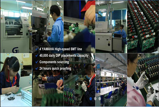
PCB ASSEMBLY CAPABILITY
| SMT service | Process capability |
| Processing type | SMT, DIP, After welding, test |
| Maximum board | L50×W50mm~L510×W460mm |
| Maximum thickness | 3mm |
| Minimum thickness | 0.5mm |
| Minimum component | 1005 |
| Maximum component size | 150mm*150mm |
| Minimum pin component spacing | 0.3mm |
| Minimum bga spacing | 0.3mm |
| Maximum component mounting accuracy(100FP) | Whole assembly accuracy up to ±50 micron,whole process repetition accuracy ±30 micron. |
| SMT capacity | 4 million pins / day |
| DIP capacity | 100 thousand/ day |