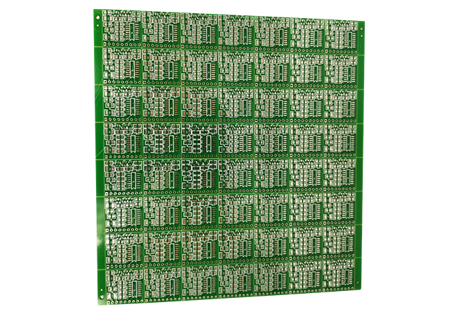
1) Thickness: 0.1mm-5mm
2) Minimum linewidth:0.075mm/3mil
3) Minimum gap:0.065/2.8mil
4) Minimum aperture inradium:0.15mm
5) Minimum aperture external diameter:0.45mm
6) Minimum BGA: 0.2mm
7) Layer:6 layers through hole non-impedance
8) PCB Assembly process: DIP, SMT, PCB Assembly
9) Item: PCBA Electronic
10) Material: Rogers; FR-4; high Tg/CTI/TD; high frequency; thick copper
All multilayer boards are printed with 36t screen, the resistance welding oil is 50 tons thicker than the traditional 43t, which provides reliability guarantee for the bga and more precise fine lines.
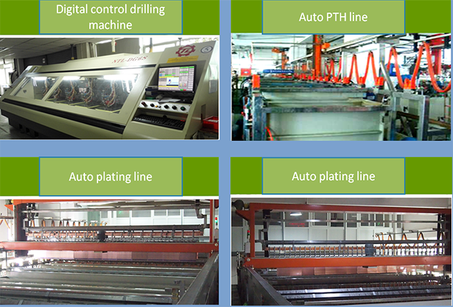
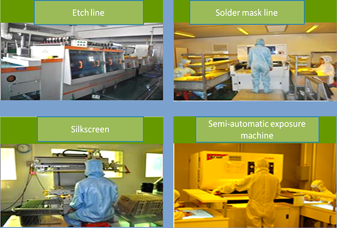
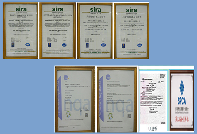
PCB fabrication FAQ
The generation of wrong size of the electric circuit board
There are many possible reasons for the wrong size. It is easy to increase and shrink in PCB production process. PCB manufacturers adjust drilling program / graphic proportion / forming CNC program, which may lead to problems such as offset of mounting, poor coordination of structural parts and so on. Because this kind of problem is difficult to detect, it can only be controlled by the PCB fabrication factory’s good process, special attention is required when selecting China PCB fabrication manufacturer.
PCB processing capability
| PCB service | Process capability |
| Layer | 1-20 layers |
| Maximum size | ≤600*500mm |
| Thickness | 0.1-5.0mm |
| Wire copper foil thickness | 17-343um(10oz) |
| Minimum linewidth / line distance | 0.075/0.065mm(3mil/2.8mil) |
| Minimum aperture | 0.15mm(6mil) |
| Minimum welding pad | 0.2mm(8mil) |
| Impedance control | +/-10% |
| Shape processing accuracy | +/-0.10mm(4mil) |
| Board type | FR-4, aluminum - base, copper -base, ROGERS, ARLON, Teflon, composite |
| Surface treatment | Tin spray, ENIG, Immerse Au, immersion silver, im mersion tin, osp, gold osp, electrospray tin |
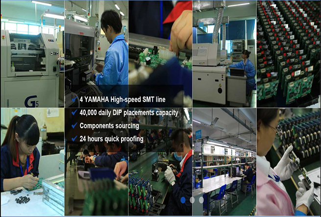
PCB ASSEMBLY CAPABILITY
| SMT service | Process capability |
| Processing type | SMT, DIP, After welding, test |
| Maximum board | L50×W50mm~L510×W460mm |
| Maximum thickness | 3mm |
| Minimum thickness | 0.5mm |
| Minimum component | 1005 |
| Maximum component size | 150mm*150mm |
| Minimum pin component spacing | 0.3mm |
| Minimum bga spacing | 0.3mm |
| Maximum component mounting accuracy(100FP) | Whole assembly accuracy up to ±50 micron,whole process repetition accuracy ±30 micron. |
| SMT capacity | 4 million pins / day |
| DIP capacity | 100 thousand/ day |