Company News
Aug. 21, 2024
3.Brown
Purpose: To form a microscopic rough and organic metal layer on the copper surface of the inner layer to enhance the adhesion between the layers.
Process principle:
Through chemical treatment, a uniform organic metal layer structure with good adhesion properties is produced, and the surface of the copper layer is controlled to be roughened before the inner layer is bonded.
4.Lamination
Lamination is the process of bonding the layers of circuits into one piece by virtue of the adhesion of the pp sheet. This bonding is achieved through the interdiffusion and infiltration of macromolecules at the interface, and then intertwined. The discrete multi-layer board and the pp sheet are pressed together to form a multi-layer board of the required number and thickness. In actual operation, copper foil, adhesive sheet (pre-hardened sheet), inner layer board, stainless steel, insulation board, kraft paper, outer steel plate and other materials are laminated according to the process requirements.
For designers, the first thing to consider when laminating is symmetry. Because the board will be affected by pressure and temperature during lamination, there will still be stress in the board after lamination is completed. Therefore, if the two sides of the laminated board are not uniform, the stress on the two sides will be different, causing the PCB board to bend to one side, which greatly affects the PCB performance.
In addition, even on the same plane, if the distribution of copper is not uniform, the resin flow speed will be different at each point, so the thickness of the place where the copper is less will be slightly thinner, and the thickness of the place where the copper is more will be slightly thicker.
In order to avoid these problems, the factors such as the uniformity of copper distribution, the symmetry of the stack, the design and layout of the blind and buried holes must be carefully considered during the design.

Pcb Board
5. Drilling
Through holes are created between the layers of the circuit board to achieve the purpose of connecting the layers.
6.Sinking copper plate
1) Shen copper
It is also called chemical copper. After drilling, the PCB board undergoes a redox reaction in a sinking copper tank, forming a copper layer to metalize the holes, and depositing copper on the surface of the original insulating substrate to achieve electrical communication between layers.
2) Plate plating
Make the PCB that has just been settled out of copper to thicken the copper in the hole to 5-8um, to prevent the thin copper in the hole from being oxidized and slightly etched away from the substrate before the pattern plating.
7. Outer dry film
The process is the same as the inner dry film.
8. Outer layer graphic plating, SES
Add holes and circuit copper layers to a certain thickness (20-25um) to meet the requirements of the final copper thickness of the finished PCB board. And useless copper on the board surface is etched away, revealing useful circuit patterns.
9. Solder mask
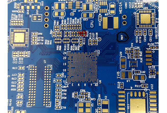
Solder mask, also known as solder mask, green oil, is one of the most critical processes in the production of printed boards. It is mainly by screen printing or coating solder mask ink, coating a layer of solder mask on the board surface, and developing by exposure. , To expose the disks and holes to be soldered, and cover the other parts with a solder mask to prevent short circuits during soldering
10. Silk screen characters
The required text, trademark or part symbol is printed on the surface of the board by screen printing, and then exposed on the surface of the board by ultraviolet irradiation.
11. Surface treatment
Bare copper itself has good solderability, but it is susceptible to moisture and oxidation when exposed to air for a long time. It tends to exist in the form of oxides, and it is unlikely to remain as copper for a long time. Therefore, the copper surface needs to be surface treated. The most basic purpose of surface treatment is to ensure good solderability or electrical properties.
12. Forming
The PCB is cut into the required external dimensions by a CNC molding machine.
13. Electrical test
The state of the simulation board, power on to check the electrical performance, whether there is open or short circuit.
14. Final inspection, spot testing, packaging
Check the appearance, size, aperture, plate thickness and marking of the board to meet customer requirements. Pack qualified products into bundles for easy storage and shipping.
We are a PCB board manufacturer. We provide high quality OSP printed circuit boards. If you have any requirements for our products, please feel free to contact us.
Previous: How Was Pcb Born?(Up)